Multicolored vertical silicon nanowires

Bulk silicon appears gray in color, though it can be made black if its reflectance is reduced by nanostructuring. Vertical silicon nanowires, however, take on a surprising variety of colors under bright-field illumination covering the entire visible spectrum. The reflection spectra each exhibit a dip, the position of which redshifts as the nanowire radius is increased, enabling fine control of the observed color. For experimental convenience, we fabricate nanowires in arrays. The spectral dip does not however arise from scattering or diffractive effects of the array, but from the waveguide mode properties of the individual nanowires. Each nanowire can thus define its own color independent of its neighbors, allowing for complex spatial patterning. This surprising phenomenon may lead to greater sensitivity in image sensor devices.

Patterned vertical silicon nanowire arrays. (a) 30º tilted SEM image of vertical silicon nanowire array pattern. Nanowires are ~1 µm long and have a pitch of ~1 µm. Letters S (left), E, A, and S (right) each comprise nanowires with radii of 70 nm, 60 nm, 50 nm and 40 nm, respectively. Bars above and below letters consist of nanowires with radii varying from 75 to 35 nm (left to right). (b) Bright-field optical microscope image of pattern. (c) Magnified image of area indicated by the white square of panel b. Each blue spot is a single nanowire. (d) 30º tilted SEM image of Bayer filter pattern. Pattern consists of vertical silicon nanowires with radii of 45 nm, 50 nm, and 65 nm representing red, blue, and green colors, respectively. Inset: magnified SEM image. Scale bar is 1 µm. (e) Bright-field optical microscope image of pattern. Each nanowire shows a color that can be controlled by appropriate choice of its radius.

This work could find applications in color image sensors based on nanowires.  Each pixel would consist of a nanowire (acting as a photodetector) formed above a second photodetector in the substrate.  Part of the spectrum would be detected by the nanowire photodetector, and part by the substrate photodetector.  In this way, one could perform color separations in an efficient manner.

Reference:

“Multicolored Vertical Silicon Nanowires,” Kwanyong Seo, Munib Wober, Paul Steinvurzel, Ethan Schonbrun, Yaping Dan, Tal Ellenbogen, and Kenneth B. Crozier, Nano Letters vol. 11, pp 1851–1856 (2011)


Surface passivation of nanowires 

Our group is interested in developing solar cells and photodetectors based on nanowires and microwires. Due to their large surface-to-volume ratios, however, nanowires have a high surface recombination rate. This can shorten the carrier lifetime by 4-5 orders of magnitude, making optoelectronic devices based on nanowires have low efficiency. Methods for the surface passivation of planar optoelectronics are well developed. The surface passivation of nanowires, however, is more challenging, due to their small size and the fact that multiple facets (with different crystalline orientations) are exposed. We have recently developed a highly effective means for surface passivation of silicon nanowires, using a thin layer of amorphous silicon formed in situ during nanowire growth (NanoLetters vol. 11, 2527 (2011)).

Silicon nanowires are synthesized by the vapor-liquid-solid (VLS) process. The amorphous surface passivation layer is formed during nanowire growth. The mechanism by which the core-shell structure (Figure 1a) is formed is still under investigation.

To characterize the surface recombination rate, we perform scanning photocurrent microscopy (Figure 1b). After making electrical contacts, the nanowire is mounted in a near-field scanning optical microscope. This enables the photocurrent, produced in response to the illumination from the aperture near-field probe, to be found as a function of probe position (Figure 1b bottom right).  The topography is found at the same time (Figure 1b bottom left).  From the photocurrent maps, the diffusion lengths are found for nanowires with different diameters (Figure 1c). Measurements are made both on core-shell nanowires, and on nanowires without shells.  From the data, we extract the surface recombination rate.  The results demonstrate that the surface recombination rate is reduced by about two orders of magnitude using the amorphous silicon coating. We further explore this phenomenon by comparing the photosensitivity of core-shell nanowires and nanowires without shells with similar diameters. These measurements are performed with light from a spectrometer, i.e. the photosensitivity is found as a function of wavelength. We find that the core-shell nanowires have photosensitivities about two orders of magnitude stronger than those of the nanowires without shells.

(a) TEM image, showing that amorphous shell is ∼10 nm thick and crystalline core is ∼40 nm in diameter. Inset: energy dispersive X-ray spectroscopy (EDS) indicates that the amorphous shell is silicon. Scale bar, 30 nm.  (b) Top: conceptual illustration of method for measuring carrier diffusion lengths.  Bottom left: nanowire topography, obtained by AFM functionality of near-field scanning optical microscope.  Bottom right: Photocurrent map, recorded simultaneously with topographic image.  (c) Surface passivation effects in nanowires of different diameters. Diffusion length vs nanowire diameter, for core-shell (black squares) and regular nanowires without shell (red dots and green stars).


Optofluidics

Our group has an interest in the integration of optics with microfluidics, a field sometimes known as “optofluidics”.  We describe below two recent examples.  In the first, we demonstrated microfluidic chips incorporating arrays of diffractive elements (zone plates) for fluorescence measurements.  In the second, we demonstrated microfluidic chips incorporating pressure sensor elements.

Fluorescence detection using an integrated zone-plate array

We have demonstrated a zone-plate array system integrated into a microfluidic device with both a large field of view and high collection efficiency, ideal for high-throughput fluorescence measurements and analysis. The design is shown in Fig. 1. A flow-focus structure generates drops, which are subsequently split and travel in 64 parallel channels. An 8-by-8 zone-plate array is aligned to the channels, with each zone plate focuses the excitation laser to a spot in one of the channelsThe fluorescence emission is collected also by the zone plates and imaged to a CCD camera. Several frames of the image stack are shown in Fig. 2. We demonstrate fluorescence measurements at up to ~184,000 drops per second. This work was published in Lab on a chip [1].

Fig. 1 Schematic of (a) the tilted view and (b) the cross section of the zone-plate array system for fluorescence detection.

Fig. 2 Frames of the collected image stack. Each zone plate observes fluorescence in drops from a different microfluidic channel.

A similar design using a zone-plate array for bead counting and sizing has also been demonstrated. The system is illustrated in Fig. 3a. The zone plates are aligned to a microfluidic channel containing fast-moving fluorescent beads. Each bead produces a peak in the fluorescent signals when it passes by the detection region of a zone plate. Fig. 3b shows a time trace of the fluorescent signals at two detection regions. The number of peaks thus represents the number of beads passing by, and the height of each peak indicates the size of its corresponding bead. This work was published in Optics Express [2].

Fig. 3 (a) Schematic of the zone-plate array system for bead counting and sizing. (b) Time trace of the signals at two detection regions.

Pressure measurements on-a-chip

We have developed an optical pressure measurement system that easily integrates into the design of microfluidic devices [3].  The sensor consists of an elastomeric membrane that is free to move up and down in response to the local fluid pressure.  These membranes are at the ends of taps leading from a main microchannel (Fig. 4a)).  The microfluidic device is placed in a microscope in transmission mode (Fig. 4b)).  In response to the pressure in the microchannel, the membrane takes on a convex shape. It thereby acts as a lens, focusing the light from the microscope’s LED. The microscope image of the sensor therefore contains a focal spot (Fig. 4b inset), whose brightness increases with pressure.  We calibrate the device by applying known pressures and recording the focal spot brightness.  It can then be used in an experiment to determine (unknown) pressures by comparing the measured brightness to that recorded in the calibration procedure.

The merits of this pressure sensing technique include 1) ease of material integration – the membrane and microfluidic chip are both made out of PDMS – alleviating bonding issues; 2) low equipment overhead – only a microscope is needed to make pressure measurements; 3) fast time response – the pressure sensing structure is extremely small (40 microns in diameter), minimizing hydraulic compliance; 4) spatial multiplexing – the small size of the sensor enables multiple sensors to be designed into the chip.  This last property enables novel visualization of pressure fields in microflows, as shown in Fig. 5.  We have also used the fast time response to detect the pressure change across a channel constriction when occupied by red blood cells – a physiologically relevant phenomenon that is understood to shed light on erythrocytic diseases such as malaria and sickle cell anemia.

Fig. 4: a) Expanded view of multilayered microfluidic device incorporating pressure sensors.  A PDMS membrane is sandwiched between two thick pieces of PDMS that define the microfluidic network.  b) Typical experimental setup showing the focusing property of the convex membrane.  Inset: CCD camera image.  Red circle denotes focal spot of a single pressure sensor.

Fig. 5: Demonstration of spatial multiplexing of pressure measurements in a microfluidic device. a)  Micrograph of a shallow flow cell with integrated pressure sensors.  b)  Pressure throughout the flow cell as reported by the membrane pressure sensors.  The device is comprised of 155 pressure sensors.


References:

[1] E. Schonbrun, A. R. Abate, P. E. Steinvurzel, D. A. Weitz, and K. B. Crozier, “High-throughput fluorescence detection using an integrated zone-plate array,” Lab Chip10, 852 (2010).

[2] E. Schonbrun, P. E. Steinvurzel, and K. B. Crozier, “A microfluidic fluorescence measurement system using an astigmatic diffractive microlens array,” Opt. Express19, 1385 (2011).

[3] Antony Orth, Ethan Schonbrun and Kenneth B. Crozier, “Multiplexed pressure sensing with elastomer membranes,” Lab on a Chip vol. 11, pp. 3810-3815 (2011)


Metasurfaces

It is an exciting time to be working in optics. Previous generations of researchers have been largely limited to the use of naturally-occurring optical materials, such as glass, crystals, et.c. Recent advances in fabrication made by the integrated circuit industry have dramatically improved our ability to produce nanostructured materials. Recent years have also seen an explosion in computing power. These two developments have made it possible to design and fabricate nanostructured materials (“metamaterials”) that have optical properties not present in natural materials. These have been used in the demonstration of several (previously unimaginable) phenomena, e.g. materials with negative refractive indices and “invisibility cloaks”. We previously demonstrated a very thin metamaterial (termed a “metasurface”) consisting of silicon nanofins on a glass substrate (Nature Comms 2014). This had the unusual property of deflecting circularly-polarised infrared light into different directions, depending on the handedness of polarisation (left- or right-handed). PhD, MPhil, & MSc projects are available on developing dielectric metasurfaces with new and technologically-useful properties. Projects will be primarily experimental, but also with theory/simulation components.


Optical forces from plasmonic and photonic devices

Integrated optical tweezers

Our group investigates integrated optical tweezers for manipulating small particles on three platforms: diffractive optics, plasmonics, and microphotonics. The incorporation of optical tweezers into microfluidic chips would provide exciting new functionalities for these systems. These include particle sorting, particle manipulation, measurement of fluid properties, and biophysical force measurements.

Manipulating microparticles using silicon photonic devices

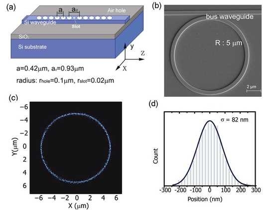
The evanescent fields of photonic devices such as waveguides, photonic crystal cavities (Fig.1a, [1]), and ring resonators (Fig.1b) can exert optical forces on particles. The gradient force due to the decaying field intensity pulls particles onto the surface where, for devices such as waveguides and ring resonators, they can be propelled by the scattering force. The planar nature of these photonic devices enables one to readily integrate multiple devices with different functionalities on the same chip. We have demonstrated optical manipulation using silicon microrings, and that the field enhancement of the cavity increases the force [2]. The particles travel around the microring, following a trajectory that deviates from circular by less than 100 nm (standard deviation, Fig1c-d).

Fig. 1 (a) 1D photonic crystal cavity with a nanoslot in the center to provide large force enhancement; (b) SEM image of microring with radius of 5 µm; (c) two dimensional histogram of the positions of a trapped particle on the microring; (d) one dimensional histogram of the particle position along radial direction.  Position = 0 nm corresponds to particle on (perfectly) circular trajectory.

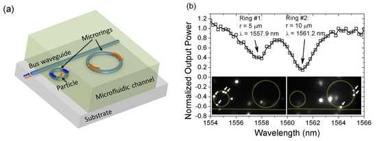
In addition to trapping and delivery, other functionalities can also be achieved using waveguide coupled devices. We have demonstrated the storage of particles (Fig. 2b) by integrating two microrings with different resonance wavelengths [3]. Tuning the laser wavelength to the resonance wavelengths of different rings enables trapped particles to be transferred back and forth between the rings. The change in output power arising from particle-induced resonance shift enables the real-time monitoring of trapped particles, such as their number and velocities, without the need for an external imaging system. The techniques we describe here could form the basis for small footprint systems in which objects are moved between multiple locations on a chip, at each of which different operations are performed and the objects’ properties sensed.

Fig. 2 (a) Schematic diagram of the microfluidic-photonic chip for sensing and storing particles; (b) Transmission spectrum of the two ring structure Inset: (left) particles are trapped by the small ring when laser wavelength is 1557.9 nm, (right) particles are trapped only on the larger ring when laser wavelength is 1561.2 nm.

Plasmonic optical tweezers

Traditional optical tweezers face difficulties at the nanoscale because of the diffraction-limited focused spot size. This has motivated interest in trapping particles with plasmonic nanostructures, as they enable intense fields confined to sub-wavelength dimensions. We have experimentally demonstrated the enhanced propulsion of gold nanoparticles by surface plasmon polaritons (SPPs) on a gold film. The field enhancement provided by SPPs and the near-field coupling between the gold particles and the film enhances the optical force [4].

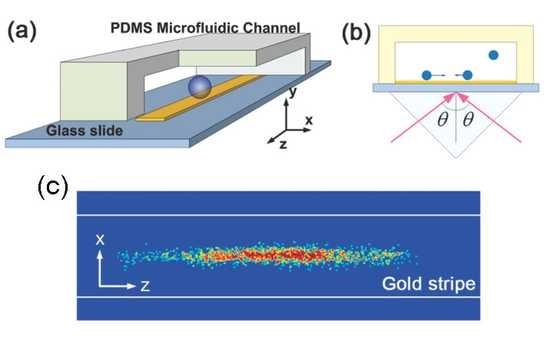
Using counterpropagating surface plasmon polaritons (SPPs) on a gold stripe, a scannable integrated optical tweezer has been achieved (Fig. 3a, [5]). Fluorescent beads are trapped and localized to the stripe center (Fig. 3c). The localization along the stripe is achieved by balancing the scattering forces from the two counter-propagating SPPs excited by prism coupling (Fig. 3b). The particle position along the stripe can be controlled by varying the relative intensity of the two input beams. This work adds an important new capability to plasmonic optical tweezers, that of scanning. We anticipate that this will broaden the range of applications of plasmonic optical manipulation.


Fig.3 (a) Schematic of plasmonic trapping device, consisting of a gold stripe in a microfluidic channel formed on a microscope glass slide. (b) Schematic of prism coupling of counter-propagating SPPs on gold stripes. (c) Measured positions of the trapped particle, recorded over a period of 1 min at 30 measurements s-1.

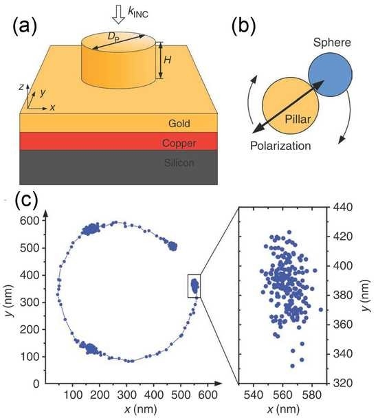
A fundamental issue with plasmonics, however, is Ohmic loss, which results in the water, in which the trapping is performed, being heated and to thermal convection. We have demonstrated the trapping and rotation of nanoparticles with a plasmonic nanotweezer consisting of a gold nanopillar protruding from a gold film (Fig.4a, [6]). The gold film, and underlying copper film and silicon substrate, act as a heat-sink drawing away the heat generated in the nanopillar by plasmon excitation. We have demonstrated the stable trapping of polystyrene particles as small as 110 nm in diameter. We have shown that particles they can be rotated around the nanopillar actively, by manual rotation of the incident linear polarization (Fig.4b-c), or passively, using circularly polarized illumination.

Fig.4 (a) Plasmonic nano-tweezer comprising nanopillar formed on gold film. Underlying copper film and silicon substrate act as heat sink, conducting heat from nanopillar to substrate, thereby minimizing water heating. Nanopillar diameter D is 280 nm, and height H is 130 nm. (b) Schematic illustration of trapping and manual rotation of nanosphere by gold nanopillar with linearly polarized illumination; (c) Left: Centroid of trapped sphere while polarization is being manually rotated. Right: centroid of trapped sphere measured without polarization rotation.

Fresnel zone plates optical tweezers

We have demonstrated that microfabricated Fresnel zone plates can be used for trapping micro-particles [7]. Fresnel zone plates are relatively simple to fabricate, making them suitable for integration into microfluidic systems. A photograph of a zone plate we fabricated is shown as Fig. 5a, and consists of concentric gold rings that block odd Fresnel zones. The zone plate is incorporated into the set-up of Fig. 5b to perform trapping. Light from a laser is collimated and illuminates the zone plate, which focuses it to a spot. Beads are trapped by the focused spot, and additional optics is used to image these beads onto a CCD. A CCD image of a trapped bead is shown as Fig. 5c. The zone plate has performance comparable to conventional optical tweezers, when its diffraction efficiency is taken into account. This work was published in Applied Physics Letters in February 2008 [7]. The integrated optical tweezers provide a tool to explore the optical force and torque on a microfluidic chip [8].


Fig. 5 a). Photo of microfabricated Fresnel zone plate. Light regions: gold. Dark regions: glass. b). Experimental set-up for trapping beads with zone plate. c). CCD image of trapped bead.

References:

[1]      S. Lin and K. B. Crozier, “Design of nanoslotted photonic crystal waveguide cavities for single nanoparticle trapping and detection,” Optics Letters, vol. 34, no. 21, pp. 3451-3453, 2009.

[2]      S. Lin, E. Schonbrun, and K. Crozier, “Optical Manipulation with Planar Silicon Microring Resonators.,” Nano letters, pp. 2408-2411, Jun. 2010.

[3]      S. Lin and K. B. Crozier, “Planar silicon microrings as wavelength-multiplexed optical traps for storing and sensing particles,” Lab on a Chip, pp. 1-5, 2011.

[4]     K. Wang, E. Schonbrun, and K. B. Crozier, “Propulsion of gold nanoparticles with surface plasmon polaritons: evidence of enhanced optical force from near-field coupling between gold particle and gold film.,” Nano letters, vol. 9, no. 7, pp. 2623-9, Jul. 2009.

[5]      K. Wang, E. Schonbrun, P. Steinvurzel, and K. B. Crozier, “Scannable plasmonic trapping using a gold stripe.,” Nano letters, vol. 10, no. 9, pp. 3506-11, Sep. 2010.

[6]      K. Wang, E. Schonbrun, P. Steinvurzel, and K. B. Crozier, “Trapping and rotating nanoparticles using a plasmonic nano-tweezer with an integrated heat sink,” Nature Communications, vol. 2, p. 469, Sep. 2011.

[7]      E. Schonbrun, C. Rinzler, and K. B. Crozier, “Microfabricated water immersion zone plate optical tweezer,” Applied Physics Letters, vol. 92, no. 7, p. 071112, 2008.

[8]      E. Schonbrun, J. Wong, and K. Crozier, “Co- and cross-flow extensions in an elliptical optical trap,” Physical Review E, vol. 79, no. 4, pp. 1-4, Apr. 2009.