Optical forces from plasmonic and photonic devices
Integrated optical tweezers
Our group investigates integrated optical tweezers for manipulating small particles on three platforms: diffractive optics, plasmonics, and microphotonics. The incorporation of optical tweezers into microfluidic chips would provide exciting new functionalities for these systems. These include particle sorting, particle manipulation, measurement of fluid properties, and biophysical force measurements.
Manipulating microparticles using silicon photonic devices
The evanescent fields of photonic devices such as waveguides, photonic crystal cavities (Fig.1a, [1]), and ring resonators (Fig.1b) can exert optical forces on particles. The gradient force due to the decaying field intensity pulls particles onto the surface where, for devices such as waveguides and ring resonators, they can be propelled by the scattering force. The planar nature of these photonic devices enables one to readily integrate multiple devices with different functionalities on the same chip. We have demonstrated optical manipulation using silicon microrings, and that the field enhancement of the cavity increases the force [2]. The particles travel around the microring, following a trajectory that deviates from circular by less than 100 nm (standard deviation, Fig1c-d).
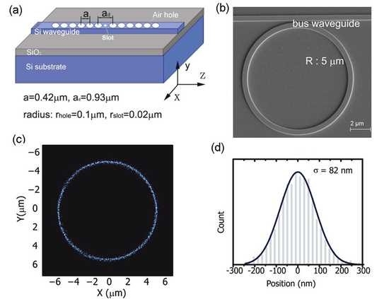
Fig. 1 (a) 1D photonic crystal cavity with a nanoslot in the center to provide large force enhancement; (b) SEM image of microring with radius of 5 µm; (c) two dimensional histogram of the positions of a trapped particle on the microring; (d) one dimensional histogram of the particle position along radial direction. Position = 0 nm corresponds to particle on (perfectly) circular trajectory.
In addition to trapping and delivery, other functionalities can also be achieved using waveguide coupled devices. We have demonstrated the storage of particles (Fig. 2b) by integrating two microrings with different resonance wavelengths [3]. Tuning the laser wavelength to the resonance wavelengths of different rings enables trapped particles to be transferred back and forth between the rings. The change in output power arising from particle-induced resonance shift enables the real-time monitoring of trapped particles, such as their number and velocities, without the need for an external imaging system. The techniques we describe here could form the basis for small footprint systems in which objects are moved between multiple locations on a chip, at each of which different operations are performed and the objects’ properties sensed.
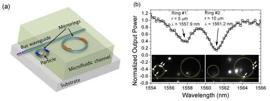
Fig. 2 (a) Schematic diagram of the microfluidic-photonic chip for sensing and storing particles; (b) Transmission spectrum of the two ring structure Inset: (left) particles are trapped by the small ring when laser wavelength is 1557.9 nm, (right) particles are trapped only on the larger ring when laser wavelength is 1561.2 nm.
Plasmonic optical tweezers
Traditional optical tweezers face difficulties at the nanoscale because of the diffraction-limited focused spot size. This has motivated interest in trapping particles with plasmonic nanostructures, as they enable intense fields confined to sub-wavelength dimensions. We have experimentally demonstrated the enhanced propulsion of gold nanoparticles by surface plasmon polaritons (SPPs) on a gold film. The field enhancement provided by SPPs and the near-field coupling between the gold particles and the film enhances the optical force [4].
Using counterpropagating surface plasmon polaritons (SPPs) on a gold stripe, a scannable integrated optical tweezer has been achieved (Fig. 3a, [5]). Fluorescent beads are trapped and localized to the stripe center (Fig. 3c). The localization along the stripe is achieved by balancing the scattering forces from the two counter-propagating SPPs excited by prism coupling (Fig. 3b). The particle position along the stripe can be controlled by varying the relative intensity of the two input beams. This work adds an important new capability to plasmonic optical tweezers, that of scanning. We anticipate that this will broaden the range of applications of plasmonic optical manipulation.
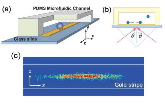
Fig.3 (a) Schematic of plasmonic trapping device, consisting of a gold stripe in a microfluidic channel formed on a microscope glass slide. (b) Schematic of prism coupling of counter-propagating SPPs on gold stripes. (c) Measured positions of the trapped particle, recorded over a period of 1 min at 30 measurements s-1.
A fundamental issue with plasmonics, however, is Ohmic loss, which results in the water, in which the trapping is performed, being heated and to thermal convection. We have demonstrated the trapping and rotation of nanoparticles with a plasmonic nanotweezer consisting of a gold nanopillar protruding from a gold film (Fig.4a, [6]). The gold film, and underlying copper film and silicon substrate, act as a heat-sink drawing away the heat generated in the nanopillar by plasmon excitation. We have demonstrated the stable trapping of polystyrene particles as small as 110 nm in diameter. We have shown that particles they can be rotated around the nanopillar actively, by manual rotation of the incident linear polarization (Fig.4b-c), or passively, using circularly polarized illumination.
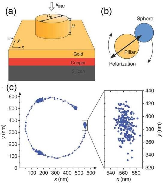
Fig.4 (a) Plasmonic nano-tweezer comprising nanopillar formed on gold film. Underlying copper film and silicon substrate act as heat sink, conducting heat from nanopillar to substrate, thereby minimizing water heating. Nanopillar diameter D is 280 nm, and height H is 130 nm. (b) Schematic illustration of trapping and manual rotation of nanosphere by gold nanopillar with linearly polarized illumination; (c) Left: Centroid of trapped sphere while polarization is being manually rotated. Right: centroid of trapped sphere measured without polarization rotation.
Fresnel zone plates optical tweezers
We have demonstrated that microfabricated Fresnel zone plates can be used for trapping micro-particles [7]. Fresnel zone plates are relatively simple to fabricate, making them suitable for integration into microfluidic systems. A photograph of a zone plate we fabricated is shown as Fig. 5a, and consists of concentric gold rings that block odd Fresnel zones. The zone plate is incorporated into the set-up of Fig. 5b to perform trapping. Light from a laser is collimated and illuminates the zone plate, which focuses it to a spot. Beads are trapped by the focused spot, and additional optics is used to image these beads onto a CCD. A CCD image of a trapped bead is shown as Fig. 5c. The zone plate has performance comparable to conventional optical tweezers, when its diffraction efficiency is taken into account. This work was published in Applied Physics Letters in February 2008 [7]. The integrated optical tweezers provide a tool to explore the optical force and torque on a microfluidic chip [8].
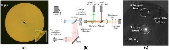
Fig. 5 a). Photo of microfabricated Fresnel zone plate. Light regions: gold. Dark regions: glass. b). Experimental set-up for trapping beads with zone plate. c). CCD image of trapped bead.
References:
[1] S. Lin and K. B. Crozier, “Design of nanoslotted photonic crystal waveguide cavities for single nanoparticle trapping and detection,” Optics Letters, vol. 34, no. 21, pp. 3451-3453, 2009.
[2] S. Lin, E. Schonbrun, and K. Crozier, “Optical Manipulation with Planar Silicon Microring Resonators.,” Nano letters, pp. 2408-2411, Jun. 2010.
[3] S. Lin and K. B. Crozier, “Planar silicon microrings as wavelength-multiplexed optical traps for storing and sensing particles,” Lab on a Chip, pp. 1-5, 2011.
[4] K. Wang, E. Schonbrun, and K. B. Crozier, “Propulsion of gold nanoparticles with surface plasmon polaritons: evidence of enhanced optical force from near-field coupling between gold particle and gold film.,” Nano letters, vol. 9, no. 7, pp. 2623-9, Jul. 2009.
[5] K. Wang, E. Schonbrun, P. Steinvurzel, and K. B. Crozier, “Scannable plasmonic trapping using a gold stripe.,” Nano letters, vol. 10, no. 9, pp. 3506-11, Sep. 2010.
[6] K. Wang, E. Schonbrun, P. Steinvurzel, and K. B. Crozier, “Trapping and rotating nanoparticles using a plasmonic nano-tweezer with an integrated heat sink,” Nature Communications, vol. 2, p. 469, Sep. 2011.
[7] E. Schonbrun, C. Rinzler, and K. B. Crozier, “Microfabricated water immersion zone plate optical tweezer,” Applied Physics Letters, vol. 92, no. 7, p. 071112, 2008.
[8] E. Schonbrun, J. Wong, and K. Crozier, “Co- and cross-flow extensions in an elliptical optical trap,” Physical Review E, vol. 79, no. 4, pp. 1-4, Apr. 2009.
Categories
One Response to “Optical forces from plasmonic and photonic devices”